

This article provides a comprehensive technical breakdown of the ESP32-P4, Espressif’s high-performance, low-power RISC-V microcontroller series. Designed for hardware engineers and IoT architects, this guide explores the architecture, electrical logic, and the critical ESP32-P4 Pinout required for professional integration.
The ESP32-P4 represents a significant leap in the Espressif ecosystem, moving beyond standard Wi-Fi/Bluetooth SoCs into the realm of high-performance microprocessors. Unlike its predecessors, the ESP32-P4 is an IO-rich, dual-system MCU designed for multimedia, edge Al, and complex industrial automation.
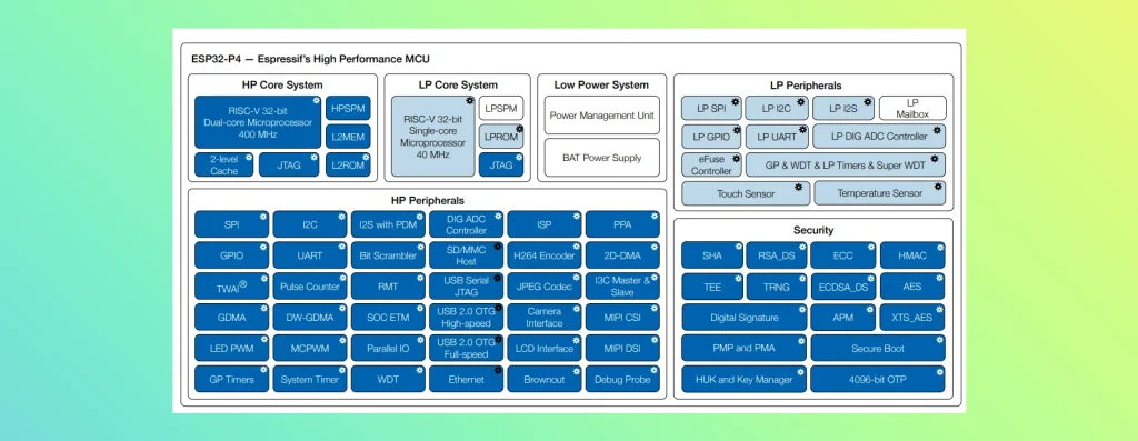
1. System Architecture: HP vs. LP Domains
The ESP32-P4 architecture is divided into two distinct power and performance domains:
2. Understanding Nomenclature and Memory Variants
It is vital to distinguish between the ESP32-P4 Series and specific part numbers. The chip name typically indicates the quantity of integrated Pseudo-Static RAM (PSRAM) within the QFN104 package
Both variants support Octal SPI (OPI) and High-speed Peripheral Interface (HPI) for data transfer.
3. Technical Deep Dive: Peripherals and Logic
Understanding the ESP32-P4 Pinout requires a grasp of how internal signals are routed to physical pins.
Analog-to-Digital Converter (ADC) Logic
The ESP32-P4 integrates two 12-bit successive approximation (SAR) ADCs capable of sampling from up to 14 pins. The ADC process involves:
UART: The Debug and Communication Bridge
Universal Asynchronous Receiver/Transmitter (UART) remains the primary serial bridge for PC-to-SoC communication. The ESP32-P4 features five HP UARTs and one LP UART. UART0 is typically mapped to GPIO37 (TXD) and GPIO38 (RXD) by default to act as the primary programming and logging interface.
4. Understanding Nomenclature and Memory Variants
It is vital to distinguish between the ESP32-P4 Series and specific part numbers. The chip name typically indicates the quantity of integrated Pseudo-Static RAM (PSRAM) within the QFN104 package
Both variants support Octal SPI (OPI) and High-speed Peripheral Interface (HPI) for data transfer.
5. Power Options and Electrical Logic
Properly energizing the ESP32-P4 Pinout is critical for stability, especially given the dual-system architecture. The SoC utilizes multiple power domains to optimize efficiency.
The Role of the LDO
Low-Dropout Regulators (LDOs) within the ESP32-P4 power scheme are essential for converting unstable input voltages into the precise 3.3V and 1.1V rails required by sensitive analog components. The LDO minimizes ripple and noise, which is paramount for the accuracy of the internal 12-bit ADCs.
WARNING: POWER SOURCE CONFLICTS Never provide power to the 3.3V pin, the 5V USB connector, and an external battery simultaneously unless your hardware includes a protection circuit (such as a Schottky diode). Simultaneous power sources can cause reverse current flow, potentially destroying the SoC or the connected power supply.
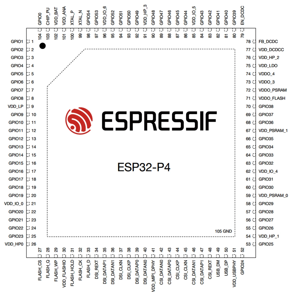
6. Detailed ESP32-P4 Pinout Tables
The ESP32-P4 uses a QFN104 package with 55 programmable GPIOs. Many pins are multiplexed via the IO MUX or the LP IO MUX.
LP GPIO and Power Management Pins
These pins are operational even when the HP system is powered down.
| Pin # | Name | Type | Function |
| 1 | GPIO1 | I/O/P | LP GPIO / ADC1_CH0 |
| 2 | GPIO2 | I/O/P | LP GPIO / ADC1_CH1 |
| 3 | GPIO3 | I/O/P | LP GPIO / ADC1_CH2 |
| 103 | CHIP_PU | I | Chip Enable (High: On, Low: Off) |
HP GPIO and Multimedia Pins
These pins support high-speed signals for cameras and displays.
| Pin # | Name | Type | Function |
| 34 | DSI_REXT | Dedicated | MIPI DSI External Resistor |
| 35 | DSI_DATAP1 | Dedicated | MIPI DSI Data Positive 1 |
| 39 | DSI_DATAP0 | Dedicated | MIPI DSI Data Positive 0 |
| 50 | USB_DP | Dedicated | USB OTG PHY D+ |
| 80 | GPIO39 | I/O | SDMMC Data 0 |
7. Programming and Boot Logic
Integrating the ESP32-P4 Pinout into a PCB design requires careful attention to Strapping Pins. These pins are sampled at the moment of boot or reset to determine the chip’s behavior.
Strapping Pins and Electrical Sampling
The ESP32-P4 uses five strapping pins to control boot modes. The most critical is the «Chip Boot Mode Control».
Firmware Download Sequence
8. References & Legal Notice
This technical manual is developed based on the official documentation provided by Espressif Systems. We highly recommend referring to the primary source for the most recent updates regarding hardware revisions and detailed specifications.
Disclaimer: ESP32 and ESP32-S2 are registered trademarks of Espressif Systems (Shanghai) Co., Ltd. This guide is an independent technical review and is not an official publication of Espressif Systems.