

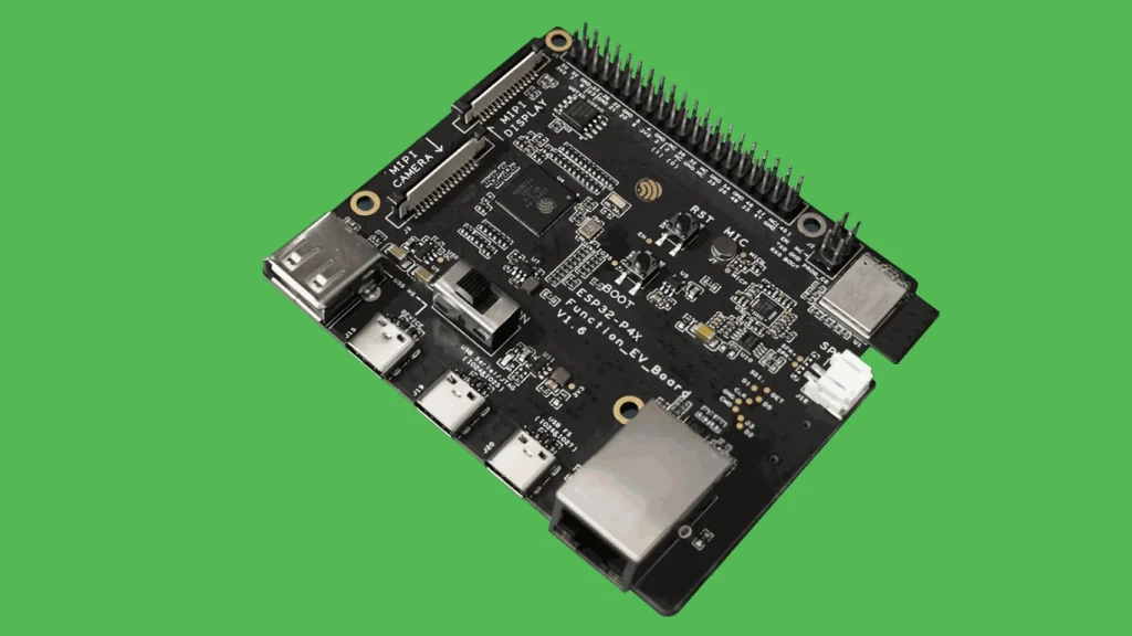
The ESP32-P4X-Function-EV-Board Pinout is the primary interface for developers looking to harness the power of Espressif’s first non-wireless, high-performance multimedia SoC. The ESP32-P4 series marks a strategic shift toward massive computational power, featuring a dual-core RISC-V architecture capable of running at 400 MHz. This specific evaluation board serves as a comprehensive development platform for advanced human-machine interfaces (HMI), integrating MIPI-CSI camera inputs and MIPI-DSI display outputs. Understanding the ESP32-P4X-Function-EV-Board Pinout is critical for hardware engineers who need to balance high-speed signal integrity with the versatile I/O requirements of modern IoT edge devices.
When discussing the architecture, it is essential to map the SoC Series versus the specific Chip Name. While «ESP32-P4» refers to the core series, the specific chip designation on your board (often found in the datasheet as ESP32-P4-WROOM or similar) typically indicates the configuration of integrated Flash and PSRAM. In the case of this EV board, the «P4» chip is a multimedia powerhouse that relies on external PSRAM (up to 32MB) to buffer high-resolution video frames. Because the chip name dictates these memory boundaries, the ESP32-P4X-Function-EV-Board Pinout must be cross-referenced with the memory bus configuration to ensure that GPIO multiplexing does not conflict with high-speed memory access.
1. Power Options and Electrical Management
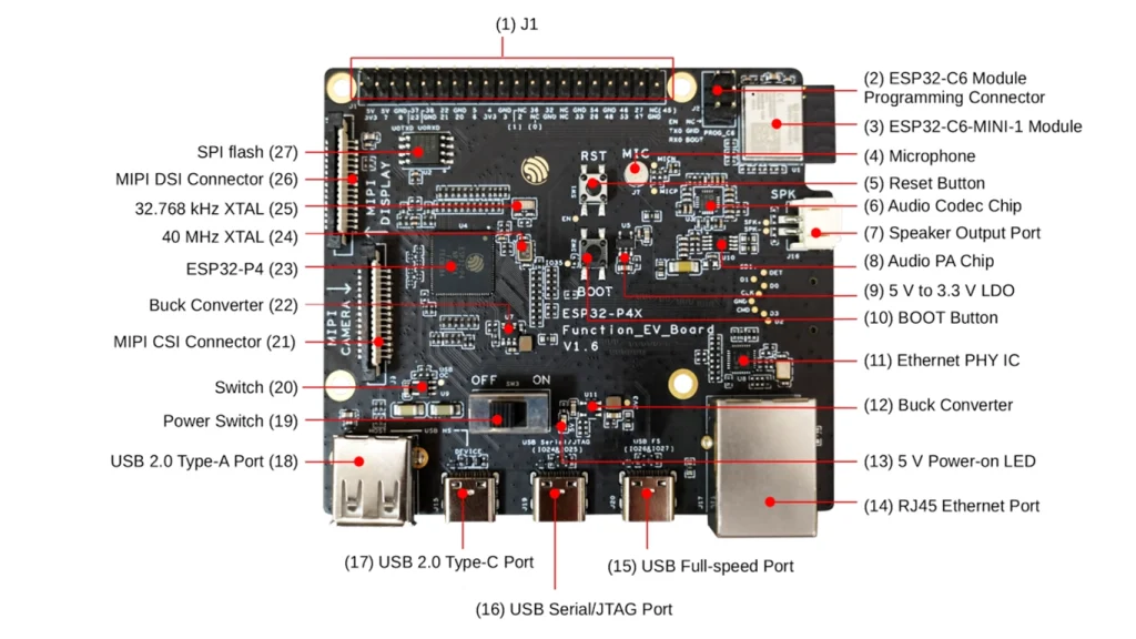
Stability in power delivery is the foundation of any high-performance system. The ESP32-P4X-Function-EV-Board Pinout provides multiple power paths: the USB 2.0 Type-C port, the Full-speed USB port, and the USB-to-UART/JTAG port. Each of these paths feeds into a sophisticated Power Management Unit (PMU). The board converts the 5V USB input into a stable 3.3V rail for the I/O pins and a 1.1V core voltage for the high-performance RISC-V cores. For multimedia applications where the 7-inch LCD backlight and camera are active, the peak current consumption can exceed 500mA, making the choice of power source critical for preventing brownout resets.
WARNING: Simultaneous Power Sources! If the USB cable used for debugging provides insufficient current, you may connect an additional 5V adapter via the secondary Type-C port. However, you must ensure that all power sources share a common ground and that no overvoltage occurs on the 3.3V rails. Failure to follow this can result in permanent damage to the ESP32-P4 silicon.
2. Technical Deep Dive: ADC Architecture
The ADC (Analog-to-Digital Converter) in the ESP32-P4X-Function-EV-Board Pinout is implemented using a SAR (Successive Approximation Register) architecture. This process is the bridge between the analog physical world and the digital processor. When an analog sensor (like a thermistor or a light sensor) is connected to an ADC-capable pin, the SAR ADC performs a binary search to find the digital equivalent of the input voltage. It compares the input against a reference voltage ($V_{ref}$) across 12 bits of resolution, resulting in 4,096 discrete levels.
Hardware implications for the ADC are significant. Since the SAR architecture relies on a capacitor array, high-impedance sources can lead to inaccurate readings if the sampling time is too short. Furthermore, because the ESP32-P4 is a high-speed digital chip, internal switching noise can couple into the ADC rails. Engineers using the ESP32-P4X-Function-EV-Board Pinout for precision measurements should implement external decoupling capacitors and use software oversampling to «average out» the thermal and quantization noise inherent in 12-bit SAR systems..
3. UART: The Communication Bridge
The UART (Universal Asynchronous Receiver-Transmitter) remains the most reliable serial interface for PC-to-SoC communication. In the ESP32-P4X-Function-EV-Board Pinout, UART0 is generally reserved for the system console and firmware flashing. Unlike synchronous protocols, UART does not use a shared clock; instead, it relies on baud rate synchronization. Each data frame is wrapped in start and stop bits, requiring both the board and the PC to have highly accurate internal oscillators to prevent bit-drift during long transmissions.
From a hardware perspective, the ESP32-P4 features dedicated hardware buffers (FIFOs) for its UART controllers. This allows the RISC-V cores to handle intense video processing while the UART hardware independently manages the serial bitstream. This offloading is vital for maintaining a responsive command-line interface (CLI) even when the system is under 90% CPU load.
4. LDO: Linear Regulation for Precision
An LDO (Low-Dropout Regulator) is utilized on the board to provide «clean» 3.3V power to sensitive analog components, such as the ES8311 audio codec. While switching regulators (Buck) are efficient, they produce high-frequency ripples that can degrade audio quality or ADC accuracy. The LDO acts as a linear filter, dropping the 5V input to 3.3V by dissipating the excess energy as heat. This thermal implication is why the ESP32-P4X-Function-EV-Board Pinout includes copper heat-sinking zones around the regulator; if the board draws too much current, the LDO can enter thermal throttling, causing the voltage rail to sag and the system to reset.
5. Strapping Pins: The Boot Logic
Strapping Pins are specific GPIOs within the ESP32-P4X-Function-EV-Board Pinout that are sampled during the reset (boot) phase. The internal ROM code checks the voltage levels on these pins to determine the «Boot Mode.» For example, if GPIO0 is pulled LOW during a reset, the chip enters Firmware Download Mode, allowing the developer to flash new code via USB. If it is HIGH, the chip attempts to boot from the integrated Flash memory.
The sampling logic happens in a matter of microseconds. This means that any external hardware connected to these pins—such as a motor driver or a sensor—must not pull the pin to an incorrect state during the power-up sequence. Mismanaging strapping pins is the leading cause of «ghost» boot failures where the chip refuses to start its application code.
6. Detailed Pinout Table (Header J1)
The following table lists the complete set of pins for the main expansion header. Every pin from the datasheet for this connector is included here without truncation.
| Pin # | Name | Type | Function |
|---|---|---|---|
| 1 | 3V3 | P | 3.3V Power Supply Output |
| 2 | 5V | P | 5V Power Supply (USB/Ext) |
| 3 | GPIO7 | I/O/T | General Purpose I/O |
| 4 | 5V | P | 5V Power Supply |
| 5 | GPIO8 | I/O/T | General Purpose I/O |
| 6 | GND | GND | Ground Reference |
| 7 | GPIO23 | I/O/T | General Purpose I/O |
| 8 | GPIO37 | I/O/T | UART0 TX / GPIO37 |
| 9 | GND | GND | Ground Reference |
| 10 | GPIO38 | I/O/T | UART0 RX / GPIO38 |
| 11 | GPIO21 | I/O/T | General Purpose I/O |
| 12 | GPIO22 | I/O/T | General Purpose I/O |
| 13 | GPIO20 | I/O/T | General Purpose I/O |
| 14 | GND | GND | Ground |
| 15 | GPIO6 | I/O/T | General Purpose I/O |
| 16 | GPIO5 | I/O/T | General Purpose I/O |
| 17 | 3V3 | P | 3.3V Power Rail |
| 18 | GPIO4 | I/O/T | General Purpose I/O |
| 19 | GPIO3 | I/O/T | General Purpose I/O |
| 20 | GND | GND | Ground |
| 21 | GPIO2 | I/O/T | General Purpose I/O |
| 22 | GPIO12 | I/O/T | Configurable IO / NC |
| 23 | GPIO02 | I/O/T | Configurable IO / NC |
| 24 | GPIO36 | I/O/T | General Purpose I/O |
| 25 | GND | GND | Ground |
| 26 | GPIO32 | I/O/T | General Purpose I/O |
| 27 | GPIO24 | I/O/T | JTAG / GPIO24 |
| 28 | GPIO25 | I/O/T | JTAG / GPIO25 |
| 29 | GPIO33 | I/O/T | General Purpose I/O |
| 30 | GND | GND | Ground |
| 31 | GPIO26 | I/O/T | LCD Backlight PWM (Default) |
| 32 | GPIO54 | I/O/T | General Purpose I/O |
| 33 | GPIO48 | I/O/T | General Purpose I/O |
| 34 | GND | GND | Ground |
| 35 | GPIO53 | I/O/T | General Purpose I/O |
| 36 | GPIO46 | I/O/T | General Purpose I/O |
| 37 | GPIO47 | I/O/T | General Purpose I/O |
| 38 | GPIO27 | I/O/T | LCD Reset (Default) |
| 39 | GND | GND | Ground |
| 40 | GPIO45 | I/O/T | Strapping Pin / GPIO45 |
7. Programming: Firmware Download Mode Sequence
To interact with the ESP32-P4X-Function-EV-Board Pinout for programming, you must master the «Boot + Reset» sequence. This forces the chip’s internal ROM to bypass the application in Flash and wait for data via the USB-to-UART bridge.
he chip is now in Download Mode. Using the ESP-IDF or esptool.py, you can now upload your binary. Once the flash is complete, a simple press of the RESET button will start your application.
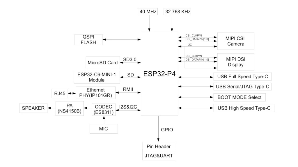
The ESP32-P4X-Function-EV-Board Pinout also interfaces with high-speed multimedia lanes not broken out to the J1 header. This includes the MIPI DSI connector for the 7-inch LCD and the MIPI CSI connector for the camera. These lanes require differential pair impedance matching (100 ohms) to function. The block diagram shows how the RISC-V dual-core CPU communicates with these blocks via the internal high-speed bus, ensuring that the heavy lifting of video processing doesn’t bottleneck the general-purpose GPIO operations.
5. References & Legal Notice
This technical manual is developed based on the official documentation provided by Espressif Systems. We highly recommend referring to the primary source for the most recent updates regarding hardware revisions and detailed specifications.
Disclaimer: ESP32 and ESP32-S2 are registered trademarks of Espressif Systems (Shanghai) Co., Ltd. This guide is an independent technical review and is not an official publication of Espressif Systems.